অন্যান্য আনুষাঙ্গিক
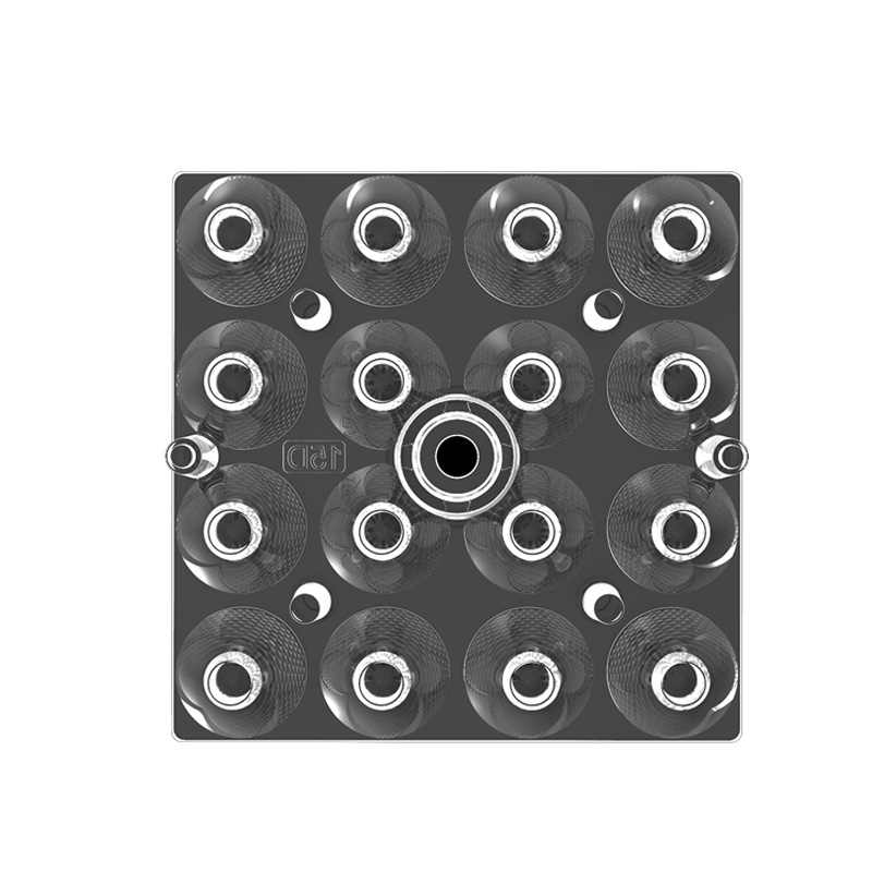
LED Street Lighting Lenses
For High Power LED Street Lights
The street light lens is specialized in high power LED street light, which can be used with high power LED.
Street Light Lens Material
- Glass lens
Because the glass material has the characteristics of high temperature resistance and high penetration rate, most of the LED street light factories are using it;
- PC or PMMA material
These two materials belong to the same class of optical plastics, can be completed through the injection molding product molding, easy to achieve aspheric light concentration, reduce the phenomenon of halo spot, the
PC and PMMA production costs have significant advantages;
Street lamp lens specifications
- Angle specifications
Generally speaking, the street lamp lens spotlight angle specifications for: 60 degrees, 80 degrees, 100 degrees, 120 degrees several kinds;
The regular road street lamp pole height of 10-12M, street lamp pole distance of 30-35M, which is deduced from the street lamp lens angle demand for 100-120 degrees
- Light spot specifications
2.1. Round spot, generally used in courtyard community roads, the irradiation range and illumination requirements are not very high.
2.2. oval spot, generally used in motor vehicles or non-motorized road, effectively eliminating the round spot irradiation, round and round on both sides of the place will have a dark area, the whole road, the light is not well distributed or a part of the round spot of light beyond the road surface and not really use it;
2.3. Rectangular light spot, applied to the motorway, the effective use of LED light, the light after the spotlight is evenly distributed on the road surface, the light spot is uniform;
PCB circuit board electronic components
PCB (Printed Circuit Board), also known as printed circuit boards, circuit boards, PCB circuit boards, etc. is an important electronic component and the support body of electronic components, also the provider of electrical connections of electronic components.
Because it is made using electronic printing technology, it is called “printed” circuit boards.
Classified according to the number of circuit layers:
Contains single-sided boards, double-sided boards and multi layer boards.
Common multi layer boards are generally 4-layer boards or 6-layer boards, complex multi layer boards can be up to a dozen layers.
Multi-layer boards (Multi-Layer Boards), which greatly increases the area that can be wired.
Multi-layer boards use several pieces of double-sided boards, and in each layer of the board into a layer of insulation between the board is glued, the number of layers of the board on behalf of the number of independent wiring layer.
Commonly, 4 to 8 layers are used, but it is technically possible to make PCB with up to 100 layers.
Line
- Minimum line width: 4mil (0.1mm), if less than 6mil line width will not be able to produce, if the design conditions permit, the larger the line width, the better the factory production, the higher the yield general design routine in 10mil or so, the design must be considered!
- Minimum line spacing: 4 mil (0.1mm)
- Line-to-outline spacing 0.508mm (20mil)
Through-hole
- Minimum hole size: 0.3mm (12mil)
- Minimum via (VIA) aperture not less than 0.3mm (12mil), pads on one side can not be less than 6mil (0.153mm), preferably more than 8mil (0.2mm).
- Via (VIA) to hole spacing (hole edge to hole edge) can not be less than 6 mil, preferably greater than 8 mil.
- Pad to profile spacing 0.508mm (20mil)


